[Thin filament pyrometry]
Main article: Thin filament pyrometry
Image of the test flame and glowing SiC fibers. The flame is about 7 cm tall.
Silicon carbide fibers are used to measure gas temperatures in an optical technique called thin filament pyrometry. It involves the placement of a thin filament in a hot gas stream. Radiative emissions from the filament can be correlated with filament temperature. Filaments are SiC fibers with a diameter of 15 micrometers, that is 5 times thinner than human hair. Because the fibers are so thin, they do little to disturb the flame and their temperature remains close to that of the local gas. Temperatures of about 800 - 2500 K can be measured.
Electronic circuit elements
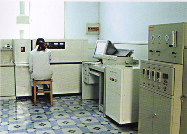
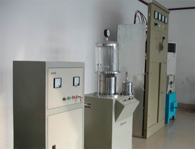
Silicon carbide is used for ultrafast, high-voltage Schottky diodes, MOSFETs and high temperature thyristors for high-power switching.[23] Currently, problems with the interface of SiC with silicon dioxide has hampered the development of SiC based power MOSFETs and insulated-gate bipolar transistors. Another problem is that SiC itself breaks down at high electric fields due to the formation of extended stacking faults, but this problem may have been resolved relatively recently.[34]
The history of SiC LEDs is quite remarkable: the first LED action was demonstrated in 1907 using SiC and the first commercial LEDs were again based on SiC. Yellow LEDs made from 3C-SiC were manufactured in in the Soviet Union in the 1970s,[35] and blue ones (6H-SiC) worldwide in the 1980s.[36] The production was soon stopped because gallium nitride showed 10-100 times brighter emission. This difference in efficiency is due to the unfavorable indirect bandgap of SiC whereas GaN has a direct bandgap which favors light emission. However, SiC is still one of the important LED components - it is a popular substrate for growing GaN devices, and it also serves as a heat spreader in high-power LEDs.[36]
Astronomy
The low thermal expansion coefficient, high hardness, rigidity and thermal conductivity make silicon carbide a desirable mirror material for astronomical telescopes. The growth technology (chemical vapor deposition) has been scaled up to produce disks of polycrystalline sililcon carbide up to 3.5 m in diameter, and several telescopes are already equipped with SiC optics.
Heating elements
References to silicon carbide heating elements exist from the early 20th century when they were produced by Acheson's Carborundum Co. in the U.S. and EKL in Berlin. Silicon carbide offered increased operating temperatures compared with metallic heaters. Silicon carbide elements are used today in the melting of non-ferrous metals and glasses, heat treatment of metals, float glass production, production of ceramics and electronics components, etc.
Nuclear fuel elements
Silicon carbide is often used as a layer of the tristructural-isotropic coating for the nuclear fuel elements of high temperature gas cooled reactors or very high temperature reactors such as the Pebble Bed Reactor. Silicon carbide provides the mechanical stability to the fuel and is the main diffusion barrier to the release of fission products.
[박판 필라멘트 고온 측정법]
시험 불꽃 과 빛나는 색의 SiC 섬유 의 이미지. 불꽃 은 약 7㎝ 높이 이다 .
탄화규소 섬유를 박판 필라멘트 고온계로 불리는 광학 기술로 가스온도를 측정하는 데 사용 된다. 그것은 고온 가스 스트림의 얇은 필라멘트의 배치를 포함한다. 필라멘트 에서 복사 배출량은 필라멘트의 온도와 상관관계가 될 수 있다. 필라멘트는 15마이크로미터 직경의 SiC 섬유인, 즉 인간의 머리카락보다 5배 더 얇다 . 그들은 불꽃을 방해하고 자신의 온도는 구간가스에 가까게 유지된다. 그러므로 약 800의 온도 - 2500K 측정 할 수 있다.
전자회로소자
탄화규소는 초고속, 고전력스위칭 고전압쇼트키 다이오드, 모스패트 및 고온사이리스터 위해 사용된다. 이산화 실리콘으로 SiC의 계면에 대한 문제가 SiC를 기반전력 모스패트의 발전을 방해하고 절연-내용게이트 바이폴라 트랜지스터. 또 다른 문제는 SiC를 자체 확장 적층결함의 형성으로 인한 높은 전기장에 장애가 있다 다만, 이 문제는 상대적으로 최근에 해결 되었다. [ 34 ]
SiC를 LED의 역사는 매우 놀라운 것입니다 : 첫 번째 LED 동작은 SiC를 사용하여 1907 년에 증명하고, 최초의 상용 LED는 다시 SiC를 기반으로 했다 . 질화칼륨은 10~100 시간을 보여 주었기 때문에 3C-SiC를 만든 노란색 LED는 1980 년대에 전 세계적으로 1970 년대에 소련에서 제조 [ 35 ]된 것과 푸른것 (6H- SiC를) 되었다. [ 36] 생산은 곧 중단되었다 밝은 빛을 방출하는 . 질화갈륨 (GaN) 발광호의 직접 밴드 갭을 가지고 있는 반면, 효율 의 차이는 SiC로 불리한 간접 밴드 갭에 의한 것입니다. 그러나, SiC를 여전히 중요한 LED 구성 요소 중의 하나는 질화갈륨 (GaN)을 분해하기위한 위한대중적인 성장 기판이고, 또한 하이파워 LED의 열 확산기로서 기능[ 36]과 천문학적인 낮은 열팽창 계수 , 높은 경도, 강성, 열전도율은 탄화규소 천체 망원경 위한바람직한 거울 소재로 이용되었다. 성장기술( 화학 기상증착)은 최대 3.5 m 직경에다 결정sililcon 카바이드의 디스크를 생산하는 최대 크기를 조정하고 있으며, 여러 망원경은 이미 SiC를 사용한 광학을 갖추고 있습니다.
탄화규소발열체
발열체는 베를린에서 미국과 EKL에서 애치슨의 카보런덤 (주)에 의해서 발견되었으며 실리콘 카바이드는 금속히터에 비해 고온의 발열온도를 제공했다. 탄화규소발열체는 비철금속 및 유리의 용해, 금속의 열처리, 플로트 유리생산, 도자기 및 전자부품의 생산, 오늘날 사용되는 핵연료의 요소와 가스원자로를 냉각 또는 페블베드 원자로 등 매우높은 온도의 원자로 고온의 핵연료 요소의 tristructural 등 방성코팅 층으로 사용된다. 탄화규소는 연료에 기계적 안정성을 제공하며, 핵분열 생성물의 방출에 메인확산 배리어 이다.